Premium content
Access to this content requires a subscription. You must be a premium user to view this content.
technical paper
Analysis of Flat-Top Nanosecond Green Laser Annealing Process for Semiconductor Si Wafers
keywords:
rapid thermal annealing
flat-top laser
semiconductor si wafer
green laser annealing
semiconductor laser applications
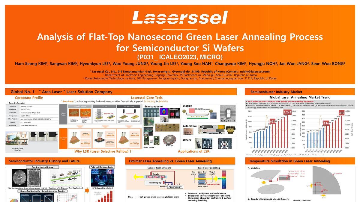
In this paper, the necessity and theoretical analysis of the flat-top nanosecond green laser annealing process are overviewed for semiconductor Si wafers. The previous technology for rapid thermal annealing on silicon wafers was based on flash ramp annealing (FLA) with uniform illumination, which involves volume heating for the entire Si wafer and uses 3–10 msec heating time. Due to the continuous technological development toward advanced semiconductor chips with narrower linewidth and pitch, top-surface-only heating demand with a very short period has been increasing to minimize the diffusion and get clear and good pattern lines. It made the development of nanosecond 532nm laser annealing technology possible, but there is a lack of information on the required energy, energy density, and relevant technological analysis. After considering the Si absorption coefficient of 7850/cm at 532nm, the specific heat capacity, the heating area of 10mm x 10mm, the heating depth of 5um, the heating volume, the heating mass, and the 4% initial reflectivity, the required pulse energy using a 1J/10nsec/532nm pulse green laser was analyzed to get various heating temperatures. Also, considering 600 ea 10mm by 10mm chips on a 300mm Si wafer, a possible ideal maximum annealing speed was calculated, which resulted in an annealing speed of one minute per wafer. Regarding green laser annealing, the technology necessity, the market trend, the power budget simulation for volume production, and the comparison to FLA are discussed.